MoTeC M48 Teardown
After working out the serial port pinout on my MoTeC M48 (see MoTeC PCI Cable for $20), I was left with one unidentified pin. As the same DB9 is used with both a PCI cable and a SUU, I suspect this extra pin is how the ECU distinguishes between the two. My M48 is already running the latest firmware so figuring out how to emulate an SUU isn’t a critical but not knowing how it works bothers me.
After trying a few things (tie pin to +5V, tie to GND), I decided I needed to open up the case and figure out where pin 12 on the ECU connector goes.
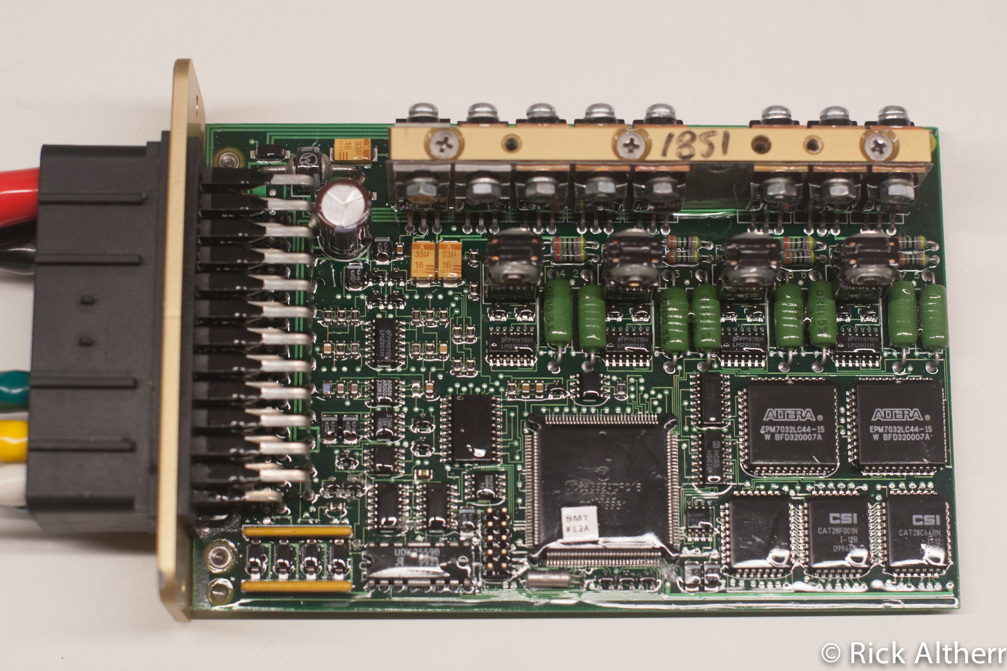
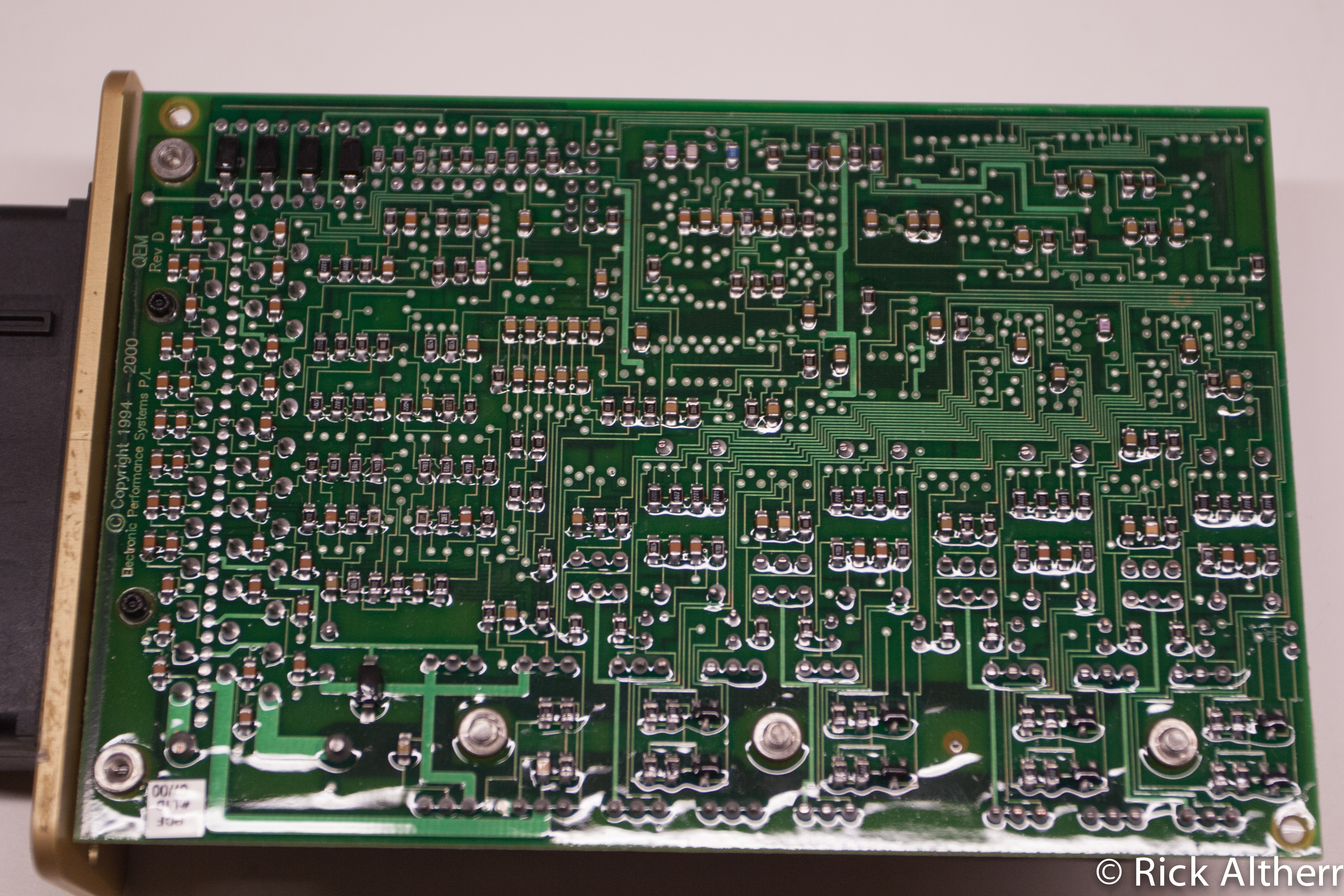
Based on the sharp, 90° bends in the traces, the whole board was definitely autorouted. Unfortunately, the autorouter decided to route traces underneath chips which makes tracing them out much harder. Also, the whole board is covered with conformal coating. On the upside, a large number of components are used to protect the inputs and output from out-of-spec voltages which makes sense as incorrect wiring is bound to be a common problem in the field.
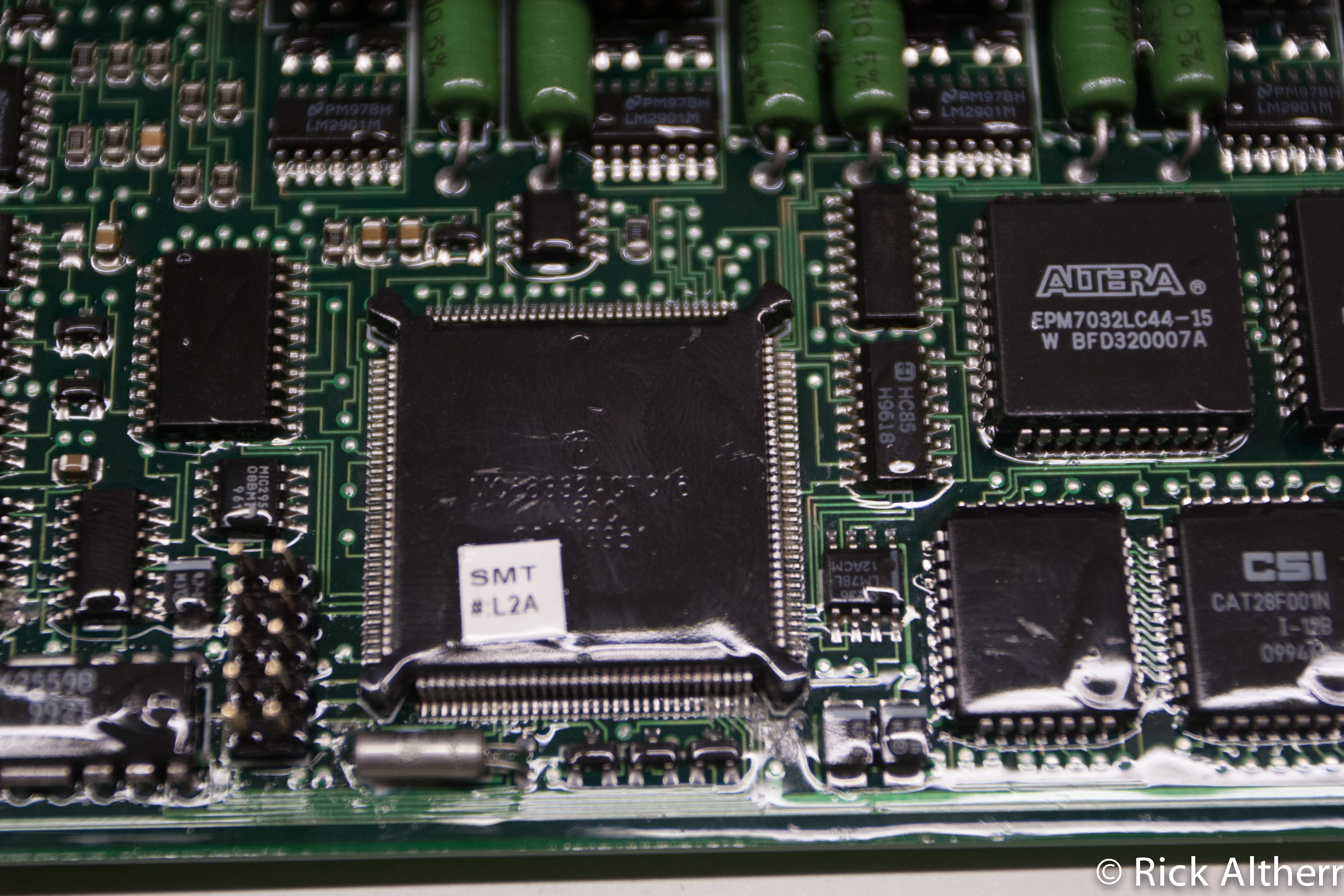
Zooming in on the main processor, I find a Motorola MC68332ACFC16 (datasheet) which is a nifty 68k variant with peripherals geared toward generating time-synchronized I/O.
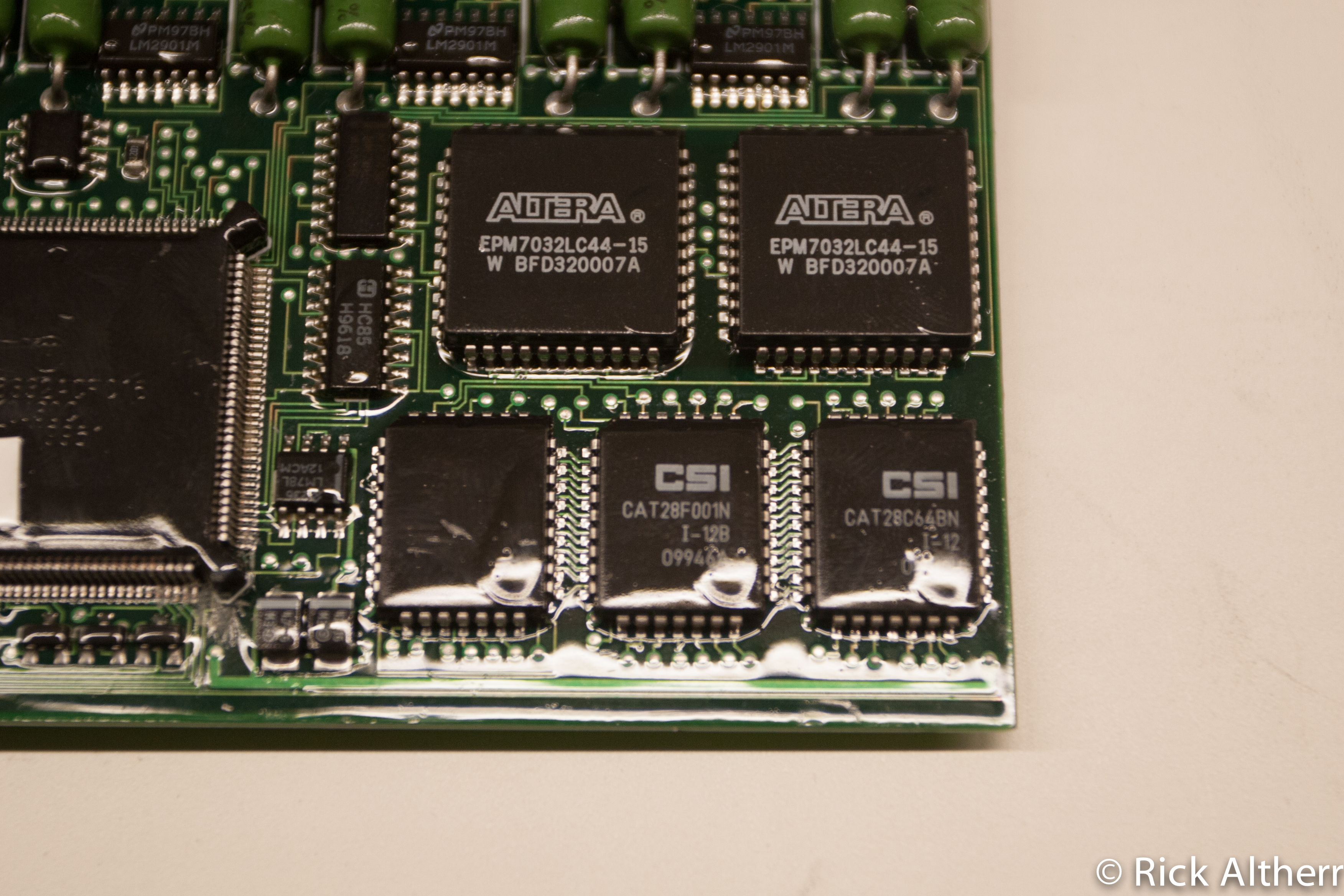
Next to the main processor are a pair of Altera MAX 7000 PLDs (EPM7032LC44 datasheet). I didn’t research enough to determine if these PLDs are used with the main processor’s time processor functions or with its expansion bus.
After a few false starts, I determined that pin 12, our extra serial pin, passes through protection circuitry before ending up at a GPIO on port E of the main processor. There seems to be no alternate functions on that pin that make sense so next up will be reverse engineering the firmware. Thankfully, MoTeC provides a full, unencrypted firmware as part of the M48 software on their website. Time to buy a license for IDA.